
Utah Nanofab
Electron Microscopy & Surface Analysis Lab
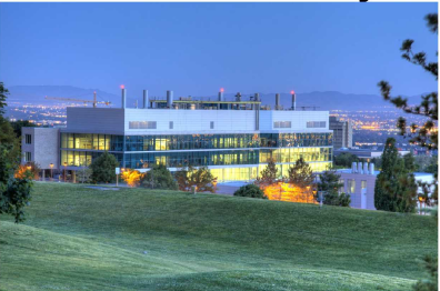
36 S Wasatch Drive
SMBB building, Suite 2500
Information
You're invited to a free tour of the Utah Nanofab Lab — exclusively organized for BIOT-8 attendees. This premier facility integrates two expert teams specializing in nano-fabrication, nano-scale surface analysis, and industrial process design. Attendees will gain rare access to advanced instrumentation and research environments that support cutting-edge innovation at the nanoscale.
This is a unique opportunity to engage directly with leading scientists and engineers, explore state-of-the-art capabilities, and deepen your understanding of applied nanotechnology in both academic and industrial contexts.
Advance registration is required, and space is limited. We encourage early sign-up to secure your place.
MULTI-SCALE Materials Characterization, Microscopy, Surface Analysis, and more!
- SEM, EDS, EBSD, TEM, STEM, hi- res XRD, MicroCT, XPS, XRF, dbFIB, AFM, LC MS, SAXS/ WAXS/GISAXS, micro-mechanical testing, nanoindentation, Ellipsometry, Profilometry, Optical Microscopy, sample prep, more!
- Elemental and chemical analysis
- Test and image/measure materials under heat, stress and strain
Industries served:
- Aerospace
- Automotive
- Battery
- Biotechnology/Health Science
- Composite Materials
- Defense
- Medical Devices
- Mining & Geo Sciences
- Nanomaterial Research
- Semiconductor
- Microelectronics
- Environmental Science